

The Final Chapter: If the Whistle Blows, Don't Fly!
M. Dennis Tierney
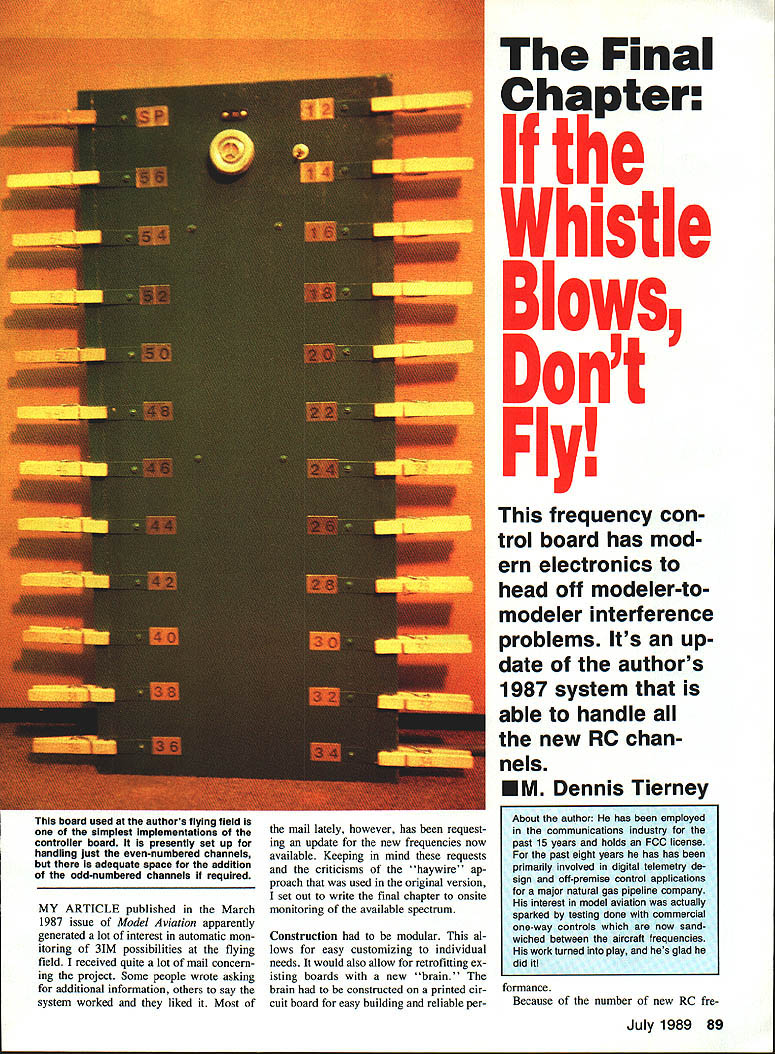
This frequency control board uses modern electronics to head off modeler-to-modeler interference problems. It's an update of the author's 1987 system that can handle all the new RC channels.
Background
My article published in the March 1987 issue of Model Aviation generated a lot of interest in automatic monitoring of 31-MHz possibilities at the flying field. I received mail asking for additional information, reports that the system worked, and many requests for an update to cover the new frequencies now available. Keeping these requests and criticisms of the "haywire" approach used in the original version in mind, I set out to write the final chapter on onsite monitoring of the available spectrum.
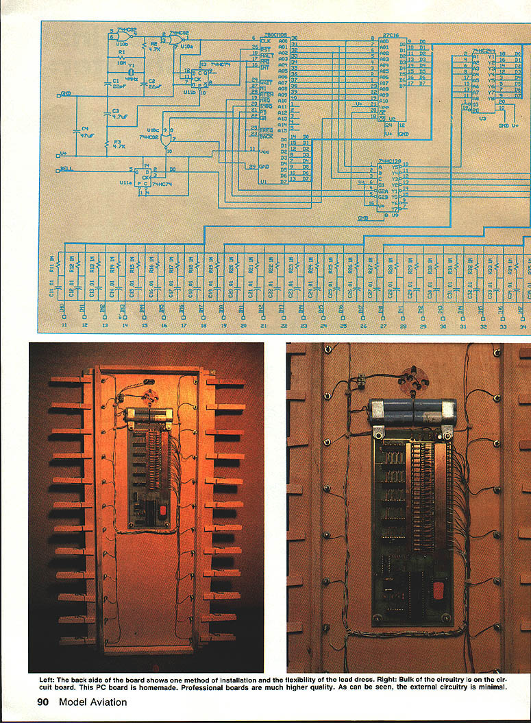
Construction had to be modular to allow easy customization and retrofitting of existing boards with a new "brain." The brain was built on a printed circuit board for easy building and reliable performance.
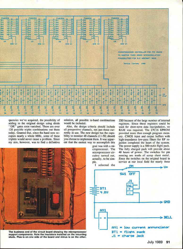
Because of the number of new RC frequencies, the possibility of expanding the original design using diode-OR gates soon vanished — there are over 120 possible triplet combinations today. Granted, since the band now occupies nearly the whole of the 30–80 MHz region, some triplets would never cause a problem. Since the aim was to find a definitive solution, all possible in-band combinations were included. The new design can monitor 48 channels (11–58).
The obvious way to accomplish the goal was with a microprocessor. Microprocessor circuitry turned out to be actually simple. I selected a Zilog Z80 because of its large number of internal registers; using registers for short-term data manipulation removed the need for RAM. A 27C16 EPROM provided enough program memory. CMOS input/output buffers, high-impedance inputs and low-pass filters for RF rejection completed the heart of the system. The power supply is a 500 mAh flight pack; a fully charged pack provides about 40 hours of power. Switches for pin sensing are made from scrap sheet metal — the switches on the original board served the local field for nearly three years, so the "ain't broke — don't fix" principle applied. Add an on-off switch and a low-current annunciator and the system is complete.
Implementation options
The implementation was left open-ended for several reasons. I visited several flying fields while traveling the Ohio River Valley and the Mississippi River Delta. One big difference among clubs is frequency control procedure. Some clubs have members place markers on the board while flying; others provide markers and remove them after flying. Some clubs require the AMA membership card to be posted to use a channel — this seems to aid recovery of markers. Clothespins are a preferred marker for convenience.
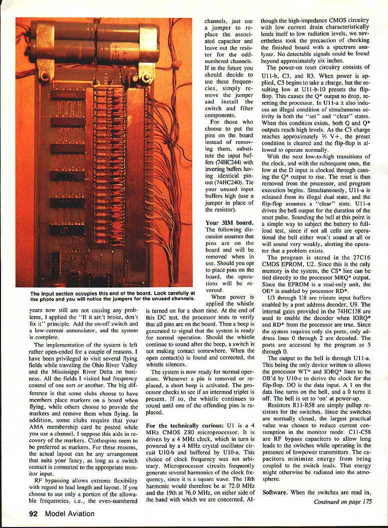
The actual layout can be any arrangement that suits your club. Long switch contacts connected to the appropriate monitor input, with RF bypassing, allow extreme flexibility regarding lead length and layout. If you choose to use only a portion of the allowable frequencies (for example, even-numbered channels), use a jumper, replace the associated capacitor, and leave out the resistor. If odd-numbered channels are required later, simply remove the jumper and install the switch and filter components.
If you prefer to put the pins on the board instead of removing them, substitute the input buffers (74HC244) with inverting buffers having an identical pinout (74HC240). Tie unused input buffers high (use a jumper in place of the resistor).
Left: The back side of the board shows one method of installation and the flexibility of the lead dress.
Right: Bulk of the circuitry is on the circuit board. This PC board is homemade. Professional boards are much higher quality. As can be seen, the external circuitry is minimal.
Your SIM board
The following discussion assumes that pins are on the board and will be removed when in use. If you opt to place pins on the board, the operations are reversed.
When power is applied, the whistle is turned on for a short time. At the end of this DC test, the processor verifies that all pins are on the board. Then a beep signals that the system is ready for normal operation. If the whistle continues to sound after the beep, a switch is not making contact somewhere; when the open contact(s) is found and corrected, the whistle silences.
The system is now ready for normal operation. Whenever a pin is removed or replaced, a short beep is activated and the processor checks for an intermod triplet. If a triplet is present, the whistle continues to sound until one of the offending pins is replaced.
For the technically curious
- U1 is a 4 MHz CMOS Z80 microprocessor. It is driven by a 4 MHz clock provided by a crystal oscillator circuit (U10-b) and buffered by U10-a. This clock frequency was chosen to avoid interfering harmonics: the 18th harmonic would be at 72.0 MHz and the 19th at 76.0 MHz, just outside the band of concern. Although the high-impedance CMOS circuitry tends to radiate very little, the finished board was checked with a spectrum analyzer; no detectable signals were found beyond approximately six inches.
- The power-on reset circuitry consists of U11-b, C3, and R3. When power is applied, C3 charges and the resulting low at U11-b pre-sets the flip-flop, causing the Q' output to drop and resetting the processor. U11-a is driven into an illegal condition of simultaneous "set" and "clear" activity; both Q and Q' reach high levels. As C3 charges to approximately 2/3 Vcc, the illegal condition clears and the flip-flop operates normally.
- With the next low-to-high transitions of the clock, the low at the D input is clocked through, causing Q' to rise and removing reset from the processor so program execution begins. Simultaneously, U11-a is released from its illegal state and drives the bell output for the duration of the reset pulse. Sounding the bell at power-up is a simple way to test the battery under load; a weak or absent bell indicates a weak battery.
- The program is stored in the 27C16 CMOS EPROM (U2). Since this is the only memory, CS* can be tied directly to the processor MRQ* output and OE* is enabled by processor RD*.
- U3 through U8 are tristate input buffers enabled by a port address decoder (U9). The internal gates of the 74HC138 are used to enable the decoder when IORQ* and RD* from the processor are true. Only six ports are required, so only address lines 0 through 2 are decoded. The ports are accessed by the program as ports 0 through 5.
- The bell output is driven by U11-a. Since this is the only device written to, the processor WR* and IORQ* lines are OR'd by U10-c to derive the clock for the flip-flop. D0 is the data input: a 1 turns the bell on, and a 0 turns it off. The bell is set to "on" at power-up.
- Resistors R11–R58 are pull-up resistors for the switches. Since the switches are normally closed, the largest practical resistor value was chosen to reduce current consumption in monitor mode. C1–C58 are RF bypass capacitors to allow long leads to the switches while operating near low-power transmitters. The capacitors minimize energy coupling to the switch leads that might otherwise be radiated.
Software
When the switches are read, their states are stored as eight-bit bytes in the processor's internal registers. For our purposes the entire string of bits can be considered a 48-bit word. The processor continuously scans the switches and compares the new input to the previously stored switch state. Any change is stored and SIM (third-order intermod, 3IM) evaluation begins.
The bell is set when the evaluation task begins. The processor applies a mask containing all possible triplets to the 48-bit pattern. The mask is oriented according to bit position; as triplets in the mask recognize that a bit is part of that triplet, 3IM evaluation proceeds.
This method requires that, at some point during evaluation, each bit be tested. To accomplish this, the entire bit pattern is shifted one position and the mask is reapplied. The process continues until 46 of the 48 bits have been shifted into bit #1 position. The remaining two shifts are not performed, since two bits cannot constitute a triplet. If no match is found, the bell is turned off and scanning continues. The execution of this process determines the duration of the beep heard when a pin is removed or replaced.
If a match is found, the bell remains on when the program returns to switch scanning. Because a change of state on a switch contact triggers evaluation, replacing any of the offending pins will produce a no-match evaluation and turn the bell off.
Construction
The full-size circuit board pattern is approximately 8.6 by 4.1 in., so an etching and drilling guide is beyond the scope of this article. I arranged with a local student coalition to provide partial kits or completely assembled and tested controllers. They will etch boards, drill, and assemble with a little help.
Pricing has been established as follows:
- 2X photo-ready etching and drilling guide — $5.00
- Custom-programmed EPROM — $12.50
- Etched and drilled printed circuit board with plated-through holes — $25.00
- Assembled and tested controller board — $100.00
Address: SJB Custom, Attn: Jason Tierney, 9788 Ralph Road, Whitesville, KY 42378. Specify that you are interested in the RC Pinboard Controller.
While this project is a bit more costly than the earlier model, its simplicity and versatility should provide a definitive solution for third-order intermod monitoring at the flying field.
Notes on layout and final remarks
Implementation was intentionally open-ended. Long switch leads can be connected to the appropriate monitor input; RF bypassing allows extreme flexibility regarding lead length. If you choose to use only even-numbered channels, use a jumper to replace the associated capacitor and omit the resistor for the odd-numbered channels. If you later decide to use the odd-numbered channels, remove the jumper and install the switch and filter components.
Happy flying!
Transcribed from original scans by AI. Minor OCR errors may remain.

